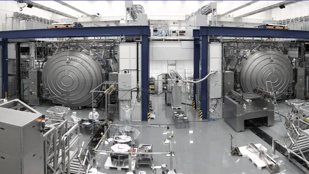
At the end of last year, ASML began delivering its first High-NA EUV (Extreme Ultraviolet) lithography system using large numerical aperture (High-NA) technology to Intel. However, it was not until recently that the CPU manufacturing giant released a video showcasing the installation process of this equipment at its facility near Hillsboro, Oregon, USA. The High-NA EUV lithography system is primarily used by Intel for research and development purposes.
Named Twinscan EXE:5000 High-NA EUV, this ASML machine is truly massive. In total, Intel requires 250 containers to transport the machine, weighing approximately 165 tons – equivalent to the weight of two Airbus A320 planes combined.
Firstly, a cargo plane transported the container from the Netherlands to Portland, Oregon, USA. Then, the components and main parts of the machine will be further transported to the facility by trucks. As you can see in the video below, the equipment has been installed at the facility, but it will take about 6 months for 250 ASML and Intel engineers to fully install the equipment.
Intel unveils video of its most advanced chip manufacturing machine
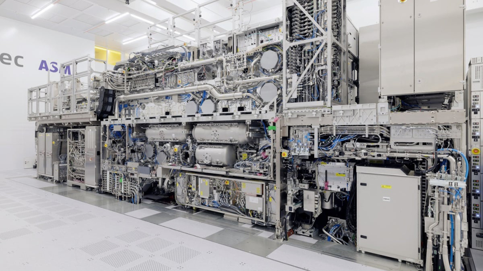
Even when the Twinscan EXE:5000 High-NA EUV machine is fully assembled, ASML and Intel engineers still need to calibrate it. This process can take a few weeks, if not months. Initially, the two companies will have to “activate” the equipment, which means when photons hit the resist layer on the wafer, something that ASML engineers recently achieved with the company’s EUV lithography system in Veldhoven, the Netherlands.
Exclusive chip manufacturing machine
Essentially, lithography is the process of printing circuit patterns onto the silicon surface of a wafer by shining light onto the silicon substrate through a pre-drawn circuit patterned glass mask. Smaller circuits require light sources with shorter wavelengths, of which EUV (Extreme Ultraviolet) light is the most advanced development to date.
A higher numerical aperture (NA) will expand the EUV beam inside the machine before it comes into contact with the silicon wafer. The wider the beam, the stronger the intensity, increasing the accuracy of the circuit printing and the component density on the silicon wafer.
Designed to enable semiconductor companies to make more complex chips, ASML’s High-NA EUV Twinscan lithography system can print lines as narrow as 8nm, significantly improving performance compared to currently used lithography systems, which are limited to 13nm with a single exposure. This breakthrough allows for semiconductor structures that are about 1.7 times smaller, resulting in nearly triple the component density. Achieving a size limit of 8nm is crucial for producing chips on a scale smaller than 3nm, a goal that the semiconductor industry hopes to achieve by around 2025 and 2026.
Intel will mainly use its Twinscan EXE:5000 High-NA EUV machine to learn how to use High-NA EUV technology. The company plans to test this lithography technology with its 18A process (although not for high-volume production) and eventually apply it to high-volume chip production with its 14A process.
Previously, ASML announced that the next-generation High-NA EUV lithography system will have a price tag twice as high as the current low-NA lithography system, amounting to around $380 million (350 million EUR). However, the exact price will depend on the specific configuration of the equipment. For example, Intel CEO Pat Gelsinger recently stated that the machine costs “about $400 million”.
By comparison, currently available low-NA EUV Twinscan NXE lithography systems cost around $183 million (170 million EUR), with variations based on specific models and configurations. While Intel may be the first company to receive this advanced chip manufacturing tool, ASML has disclosed that it has received “between 10 and 20” orders for their High-NA EUV machines from companies such as Intel, Samsung, SK Hynix, and TSMC.
ASML began as a subsidiary of the Dutch electronics giant Philips in 1984. They introduced their first lithography machine – invented in a US military laboratory in the 1950s – from a storage warehouse adjacent to a Philips office building in Eindhoven, the Netherlands. By 1988, ASML had 5 US offices with 84 employees and a new office in Veldhoven, the Netherlands, which eventually became the company’s headquarters.
ASML has sold a total of about 140 EUV systems in the past decade, each system priced up to $200 million, according to Wennink. Starting in 2018, the administration of former US President Trump is believed to have pressured ASML not to sell EUV technology to Chinese companies.


